PCB Fail
Ever since first trying KiCad and OSH Park I have been a little hooked on being able to throw together a custom PC, have it professionally manufactured, and shipped to me within a couple weeks. We’ve used KiCad and OSH Park on all of our prototypes here at Maniacal Labs but Dan and I use them constantly for our own projects as well. It’s quick and cheap, but I recently discovered the hard way not to go too quickly.
I was designing a PCB for a custom LED strip controller for a costume piece I’m working on. Nothing overly complicated, just an ATMega1284p, a button, rotary encoder, OLED screen, and a few capacitors and resistors. I had already breadboard the entire circuit and was confident it would work, so I decided to throw together the PCB and get it ordered.
Since I already had a design for an ATMega1284p breakout board I had design and used, I started with that, removed the parts I didn’t need and added in the button, encoder and screen. But re-using this design was also where I went a little wrong. KiCad has a feature called a “net name” where you can just drop a little tag on a component pin, name it, and all other tags with the same name will be connected automatically in the PCB routing. It’s a really great way to de-clutter your schematic.
However, my original breakout board design had a net named “RST” which was for the ATMega RESET pin, that gets hooked up to the FTDI & ICSP headers and pulled to VCC through a 10k ohm resistor. The problem came when I added in a schematic component for my OLED screen (a great one from Adafruit) which has a pin labeled “RST”. I needed this pin, so when I created its net name I, of course, named the net for that pin “RST”. A quick look at the design seemed enough to convince me that everything looked okay. So, after only about 25 minutes work, I sent the design to OSH Park to be fabricated.
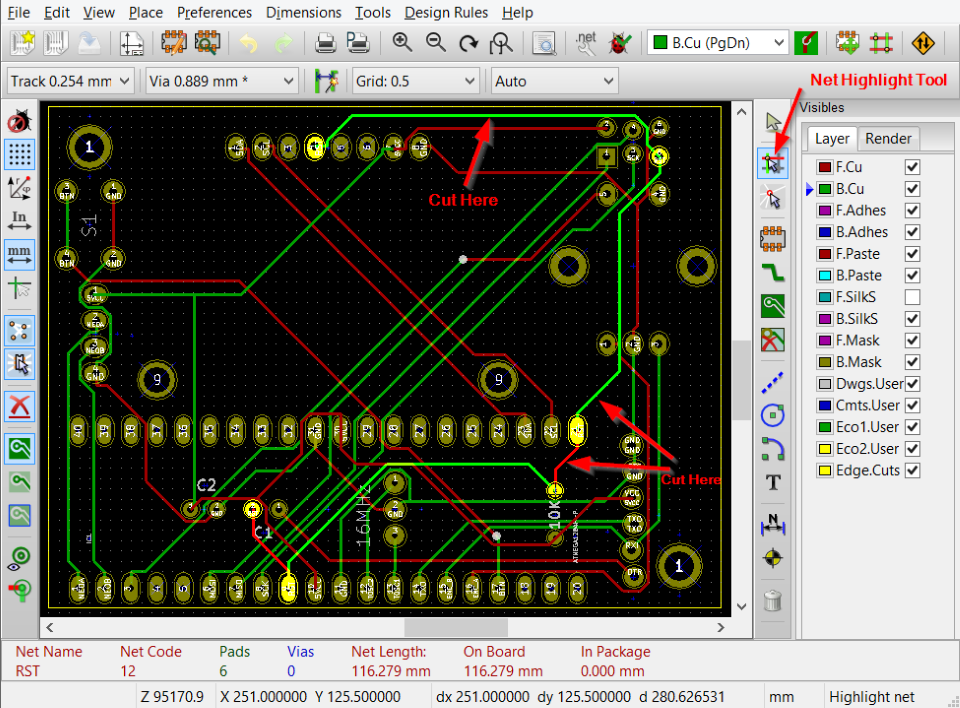
Fast forward to yesterday. I got the boards back, solder everything on, power it up (the chip was already flashed), and… nothing. No screen display, no serial output. I tried flashing the firmware again only to find that my computer could not communicate with the chip. So, I did what I should have done in the first place. Went back to the PCB designs and used the “highlight net” tool to see what was hooked up wrong.
I quickly realized that RST on the OLED screen was connected to ATMega RESET pin. You can see the offending net brighter than the rest. The OLED RST pin is supposed to be only hooked up to PD7 on the ATMega so it can be reset from firmware. Without having a schematic for the OLED it’s hard to say, but my suspicion is that the OLED RST pin is pulled to ground internally to default to a reset state and expects to be pulled high by the micro-controller. Therefore it was was holding the ATMega RESET pin low and preventing it from booting.
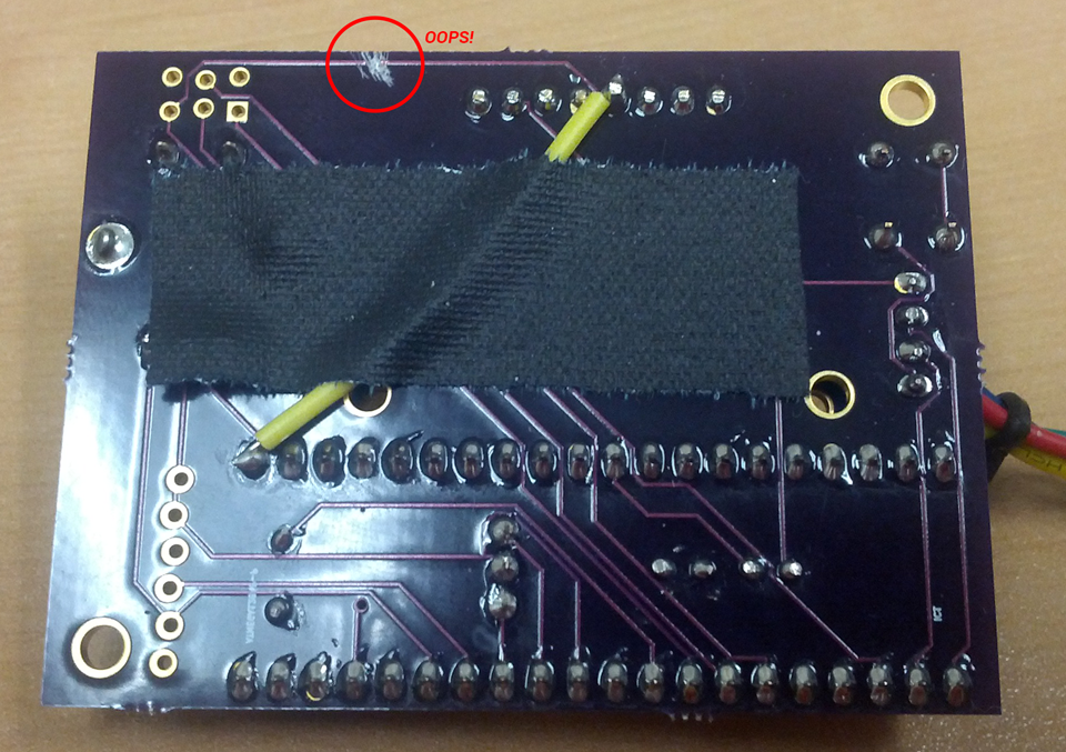
Fortunately, the fix was simple enough. Scrape away the offending PCB trace (as seen in the screenshot) and solder in a wire from the ATMega pin PD7 to the OLED itself. You can see my fix in the top image.
So, lesson learned. Always, always, double and triple check your schematic and PCB nets before sending a design off to be fabricated. Better yet, don’t design a board in less than 30 minutes and then order immediately if it happens to be 1am. Wait until the morning. You might notice a mistake or two ;)


